Measured CMOS timer standby currents and supply-range robustness can be an order of magnitude better than legacy bipolar 555s, motivating designers to choose low‑power CMOS alternatives for battery‑sensitive timing and pulse generation. This article translates the ICM7555 datasheet into practical guidance on pinout, electrical specs, limits, and real‑world design constraints, helping engineers move from sheet data to validated bench designs. (Keywords: ICM7555, datasheet, pinout.)
Point: provide compact, actionable translation of vendor datasheet specifics. Evidence: consolidated comparator thresholds, quiescent currents, and absolute limits drive choices in component selection. Explanation: readers will get pin‑level behavior, timing math with numeric examples, layout and test checklists, and common failure mitigations applicable to low‑power CMOS timers.
1 — Why the ICM7555 Matters: Background & Use Cases
1.1 Typical application domains
Point: The device excels in monostable delays, astable oscillators, PWM sources, watchdogs, LED timing, and ultra‑low‑power timers. Evidence: low quiescent current and rail‑to‑rail tolerant thresholds enable multi‑cell battery and low‑voltage designs. Explanation: choose this CMOS timer when minimal standby drain and small component count matter; prefer discrete or precision op‑amp timing where ppm accuracy or very long time constants are required.
1.2 Key functional differences vs. legacy bipolar timers (high level)
Point: CMOS architecture reduces supply current and expands recommended supply range versus bipolar counterparts. Evidence: internal CMOS comparators and lower bias currents yield markedly reduced quiescent current and improved input threshold stability. Explanation: benefits include longer battery life and simpler power margining; trade‑offs include potentially lower output drive and different output stage behavior under heavy inductive/capacitive loading.
2 — ICM7555 Pinout & Functional Block Overview (Pinout-focused; contains keyword)
2.1 Pin-by-pin breakdown (what each pin does)
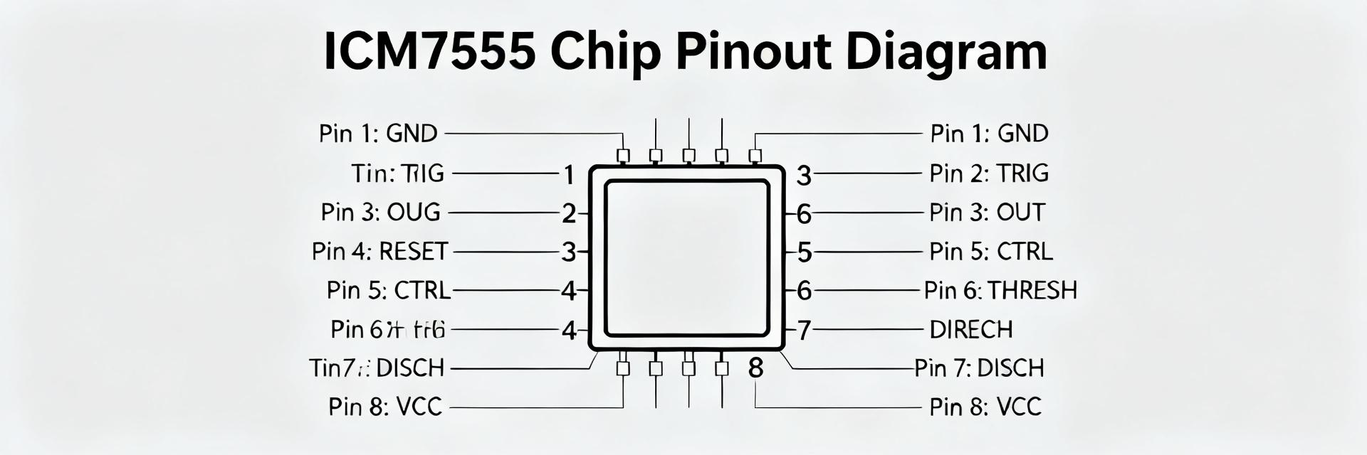
Point: each of eight pins has defined roles: VCC (pin 8), GND (pin 1), TRIG (pin 2), OUT (pin 3), RESET (pin 4), CTRL (pin 5), THRS (pin 6), DISCH (pin 7). Evidence: typical behavior—TRIG is active low comparator input, THRS senses capacitor voltage, DISCH is open‑collector/transistor to ground, CTRL sets internal 2/3 VCC reference. Explanation: expect high input impedance on TRIG/THRS, limited source/sink at OUT (sized for logic loads), and recommend buffering heavy loads or using a series resistor with capacitive loads to protect DISCH.
| Pin | Name | Function / Typical Behavior |
|---|---|---|
| 1 | GND | Ground reference; return for supply and discharge transistor |
| 2 | TRIG | Active‑low trigger comparator input; high impedance |
| 3 | OUT | Push‑pull output; limited drive—buffer for >10 mA |
| 4 | RESET | Active‑low reset; tie high for normal operation |
| 5 | CTRL | Control voltage input (nominal 2/3 VCC); decouple for stability |
| 6 | THRS | Threshold comparator input; senses timing cap voltage |
| 7 | DISCH | Open‑collector transistor to ground for capacitor discharge |
| 8 | VCC | Supply; recommended decoupling close to pin |
2.2 Internal functional blocks & signal flow
Point: internal comparators, an RS flip‑flop, discharge transistor, and output stage implement timing. Evidence: trigger/threshold comparators toggle the flip‑flop at ~1/3 and ~2/3 of VCC, with CTRL pin allowing external adjustment. Explanation: during monostable operation a trigger pulses the flip‑flop, DISCH releases the timing capacitor to charge via R until THRS trips; in astable mode the flip‑flop toggles continuously producing oscillation.
3 — Electrical Specifications & Absolute Limits (Data deep-dive; contains keyword)
3.1 Recommended operating conditions vs. absolute maximums
Point: design within recommended VCC range and temperature limits, and margin from absolute maximums. Evidence: recommended supplies typically span a low‑voltage region up to mid‑tens of volts; absolute max supply and input voltages exceed recommended by a safety margin. Explanation: follow derating—design at least 10–20% below absolute limits, add transient suppression and supply sequencing to prevent latch‑up and reliability loss under stress.
3.2 Key electrical parameters: currents, thresholds, timing tolerances
Point: focus on quiescent current, output drive, comparator thresholds, discharge transistor on‑resistance, and capacitor leakage. Evidence: quiescent currents are typically microamps to low hundreds of microamps; thresholds center near 1/3 and 2/3 VCC, and timing accuracy is affected by supply variations and capacitor leakage. Explanation: use the timing formula sensitivity to VCC to estimate frequency drift; when long pulses are needed, select low‑leakage capacitors and allow margin for worst‑case threshold shifts.
4 — Timing Calculations & Design Guidelines (Method / how-to)
4.1 Monostable & astable formulas with worked examples
Point: monostable pulse width t ≈ 1.1·R·C; astable high time tH ≈ 0.693·(RA+RB)·C, low time tL ≈ 0.693·RB·C. Evidence: numeric example—monostable with R=100kΩ and C=1µF yields t≈0.11 s; astable with RA=10kΩ, RB=100kΩ, C=0.01µF gives f≈1/[0.693·C·(RA+2RB)] ≈ 1.25 kHz. Explanation: include resistor tolerances and capacitor tolerance in worst‑case timing budgets; control pin variance and supply ripple will shift thresholds and thus timing, so budget ±10–20% for general use or choose precision components for tighter specs.
4.2 Layout, bypassing, and stability tips
Point: PCB layout and decoupling directly affect jitter and stability. Evidence: a 0.01–0.1µF ceramic decoupler at VCC to GND placed within 2–5 mm of the package dramatically reduces supply transient coupling; CTRL pin decoupling with 10 nF stabilizes reference. Explanation: minimize ground loops, run timing capacitor return close to GND pin, avoid routing noisy traces near TRIG/THRS, and prefer C0G/NP0 or polypropylene caps for precision timing to reduce dielectric absorption.
5 — Typical Application Circuits & Limit Conditions (Case studies)
5.1 Common reference circuits to include and analyze
Point: typical circuits are monostable delay, astable LED flasher, PWM dimmer, and low‑voltage start‑up. Evidence: monostable sketch uses single R and C on TRIG/THRS with RESET tied high; astable uses two resistors and one capacitor between DISCH/THRS. Explanation: for LED flasher expect a few mA drive; for PWM dimmer use OUT to drive a logic FET or driver; for low‑voltage start‑up ensure VCC and RESET sequencing so the device initializes reliably at supply ramp.
5.2 Stress scenarios and limits (voltage spikes, load extremes, temperature)
Point: stress cases include heavy capacitive loads, negative transients on inputs, and high‑temperature drift. Evidence: driving large capacitive loads increases DISCH switching losses and may pull VCC during transitions; negative transients on TRIG/RESET can forward‑bias internal structures. Explanation: mitigate with series resistors, clamp diodes on inputs, small RC snubbers on outputs, and thermal margining—limit ambient operating temperature and derate supply to preserve long‑term reliability.
6 — Testing, Troubleshooting & Best Practices (Action-oriented)
6.1 Bench test checklist & measurements to validate design
Point: perform a standard verification sequence: supply ramp, trigger threshold sweep, frequency sweep, output drive under load, and quiescent current measurement. Evidence: measure quiescent current with a µA‑range meter at nominal VCC, probe thresholds with a scope and high‑impedance probe, and validate timing against formula under worst‑case tolerances. Explanation: use proper probe grounding, remove scope ground loops, and verify with short‑circuit and hot‑temperature tests before production.
6.2 Common failure modes and quick fixes
Point: symptoms include unstable frequency, no output, stuck states, or excessive standby current. Evidence: common causes are missing decoupling, miswired pins, leaky timing capacitors, or improper RESET/CTRL handling. Explanation: remedies include adding local decoupling, verifying pin connections, replacing electrolytic timing caps with low‑leakage types, and adding pull‑ups or pull‑downs to undefined control pins.
Summary
Understanding the ICM7555 pinout and datasheet electrical specifications enables confident deployment of low‑power CMOS timers in battery and logic applications. Designers should margin supply and temperature ratings, choose low‑leakage timing components, and apply layout decoupling best practices before scaling to production. Test on the bench with the suggested checklist and validate timing against worst‑case component tolerances and vendor datasheet figures for robust results. (Keyword: ICM7555N)
Frequently Asked Questions
What is the main advantage of the ICM7555 over the standard NE555?
The ICM7555 uses CMOS technology, resulting in significantly lower quiescent current (microamps vs. milliamps), higher input impedance, and rail-to-rail output swing, making it ideal for battery-sensitive applications.
How do I calculate the monostable pulse width for the ICM7555?
The monostable pulse width t is approximately 1.1 × R × C, where R is the timing resistor in ohms and C is the timing capacitor in farads. Ensure you account for component tolerances.
Why is decoupling critical for the CTRL pin (Pin 5)?
The CTRL pin sets the internal voltage reference. Noise or instability here directly affects comparator thresholds, leading to timing jitter or false triggering. A 10nF ceramic capacitor to ground is recommended.
Can the ICM7555 drive heavy loads directly?
While the output stage is push-pull, its current drive capability is limited compared to bipolar versions. For loads exceeding ~10mA or highly capacitive/inductive loads, use a buffer transistor or MOSFET.


